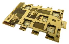
RF Circuit Board Design
Achieving high-quality RF circuit boards requires careful design, fabrication, and testing. Common RF PCB reliability issues include signal loss and interference, which degrade the quality of transmitted or received signals. These issues can be mitigated through PCB material selection and manufacturing controls that minimize sources of noise and distortion.
High-frequency signals can be impacted by a number of factors, including impedance mismatches in transmission lines and component connections, skin effect (current tending to flow on the surface of conductors), and cross-talk (signals from adjacent traces or components that inadvertently couple with each other). To avoid these problems, designers must carefully plan the placement of rf circuit board design components and minimize the distances that signals must travel to reduce loss and interference.
RF PCBs must also feature a ground plane, which serves as a low-impedance reference for the signals on an adjoining layer. The ground plane also prevents unwanted reflections and resonant frequencies from causing interference between signals and components.
Limitations of RF Circuit Board Design
To ensure proper impedance matching, a RF PCB must have its conductors and dielectric layers of a specific size and shape. A larger conductor’s diameter offers a lower impedance and higher performance than a smaller one, while the aspect ratio of the via’s diameter/depth must be appropriate to avoid high parasitic capacitance or inductance.
Impedance matching is especially important in RF applications, since high-frequency signals require precise tolerances to maintain performance. This means that RF PCBs need to be manufactured using a variety of materials, each with a specific dielectric constant, loss tangent, and coefficient of thermal expansion that meets the demands of the targeted application. For example, if a PCB is intended for use in a high-frequency satellite communication system, it must be made from ceramic materials with low dispersion and phase shift.
PCB manufacturing for RF circuits can be difficult due to the high-frequency, complex nature of the board’s layout and its requirements for precision impedance matching. This can result in a significant amount of test and validation time to ensure that the circuitry is working correctly. Common tests that are performed on RF PCBs include network analysis and time-domain reflectometry, which help to determine how well the RF circuit board performs in its intended environment.
When creating an RF circuit board, it’s also important to consider the durability of the plated through holes (PTHs) that connect the traces and components. The integrity of these holes is crucial to the reliability of a circuit board in a harsh environment, such as space. To ensure this, RF PCBs should be manufactured with standard and specialty equipment that can produce PTHs that are durable enough to withstand temperature cycling and thermal extremes in space. This includes plasma etch machinery and laser direct imaging (LDI), which helps to maintain quality with minimal variation in trace width and front-to-back registration.